(China (Mainland))

Product Summary
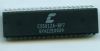
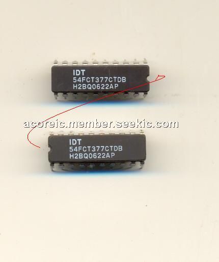
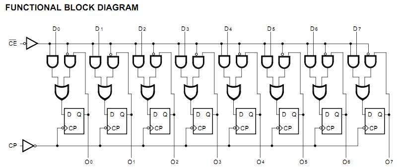
The IDT54FCT377CTDB is an octal D flip-flop using an advanced dual metal CMOS technology. The IDT54FCT377CTDB has eight edge-triggered, D-type flip-flops with individual D inputs and O outputs. The common buffered Clock (CP) input loads all flip-flops simultaneously when the Clock Enable (CE) is LOW. The register is fully edge-triggered. The state of each D input, one set-up time before the LOW-to-HIGH clock transition, is transferred to the corresponding flip-flop’s O output. The IDT54FCT377CTDB CE input must be stable only one set-up time prior to the LOW-to-HIGH transition for predictable operation.
Parametrics
IDT54FCT377CTDB absolute maximum ratings: (1)VTERM, Terminal Voltage with Respect to GND: –0.5 to +7.0V; (2)VTERM, Terminal Voltage with Respect to GND: –0.5 to VCC +0.5V; (3)TA, Operating Temperature: 0 to +70℃; (4)TBIAS, Temperature Under Bias: –55 to +125℃; (5)TSTG, Storage Temperature:–55 to +125℃; (6)PT, Power Dissipation: 0.5W; (7)IOUT, DC Output Current: –60 to +120mA.
Features
IDT54FCT377CTDB features: (1)Std., A, C and D speed grades; (2)Low input and output leakage ≤1μA (max.); (3)CMOS power levels; (4)True TTL input and output compatibility: VOH = 3.3V (typ.); VOL = 0.3V (typ.); (5)High drive outputs (-15mA IOH, 48mA IOL); (6)Power off disable outputs permit live insertion; (7)Meets or exceeds JEDEC standard 18 specifications; (8)Product available in Radiation Tolerant and Radiation Enhanced versions; (9)Military product compliant to MIL-STD-883, Class B and DESC listed (dual marked); (10)Available in DIP, SOIC, QSOP, CERPACK and LCC packages.
Diagrams
 |
 IDT54 |
Other |
|
Data Sheet |
Negotiable |
|
||||
|
IDT54/74FCT646 |
Other |
|
Data Sheet |
Negotiable |
|
||||
|
IDT54/74FCT646A |
Other |
|
Data Sheet |
Negotiable |
|
||||
|
IDT54/74FCT646C |
Other |
|
Data Sheet |
Negotiable |
|
||||
|
IDT54/74FCT827A |
Other |
|
Data Sheet |
Negotiable |
|
||||
|
IDT54/74FCT827B |
Other |
|
Data Sheet |
Negotiable |
|
||||